
Fichier:MicroChipAtomicTrap00.jpg

Fichier d’origine (890 × 976 pixels, taille du fichier : 44 kio, type MIME : image/jpeg)
Ce fichier et sa description proviennent de Wikimedia Commons.
| Description |
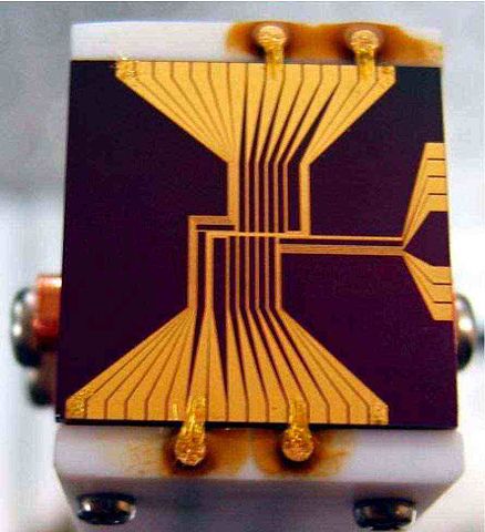
The first microchip atomic trap, designed at the Institute for Laser Science, Japan. The structure of wires is painted with gold at the insulator substrate. The main wire has Z-shape; the magnetic field allows the trapping of neutral atoms due to their magnetic momentum. The ship has sizes 2 x 2 cm. It was placed to the uniform magnetic field (source of this field is not shown in the figure); the traping is realized for so-called "atoms seeking for low magnetic field". The only atoms with positive spin-field energy were trapped. The miminim of the field is realized at the side of the chip, close to the central part of the z-electrode with electric current. This movement is limited by the edges of the "Z". Additional electrodes were designed to allow the play with the effective potential along this wire; the interaction with laser beams and reduction of the trapping potential allow the additional cooling of atoms (coling with vaporation), reaching the BEC. In the current design, the only one additional electrode is supplied with contacts. It was planned to use other electrodes to modify the potential in experiments with single-dimentional quantum mechanics. Actually, more advanced microchip atomic traps were manufactured instead. |
| Date | y.2003 |
| Source | private communication |
| Auteur | Ken-Ichi Nakagawa |
| Autorisation (Réutilisation de ce fichier) |
copuleft directly from author |
| Autres versions |
Up to my knowkedge, it is the best resolution image of the First Microship Atomic Trap, ever posted. lower resolution pics are available at
|

|
Le détenteur des droits d’auteur de ce fichier autorise n’importe qui à l’utiliser pour n’importe quelle utilisation, pourvu que le détenteur des droits d’auteur soit correctement attribué. La redistribution, les œuvres dérivées, l’utilisation commerciale et toutes les autres utilisations sont autorisées. |
|
|
Links
Historique du fichier
Cliquer sur une date et heure pour voir le fichier tel qu'il était à ce moment-là.
| Date et heure | Vignette | Dimensions | Utilisateur | Commentaire | |
|---|---|---|---|---|---|
| actuel | 12 septembre 2007 à 05:47 | | 890 × 976 (44 kio) | Domitori | {{Information |Description=The first microchip atomic trap, designed at Institute for Laser Science, Japan. The main wire has Z-shape; the magnetic field allows the trapping of neutral atoms due t |
Utilisation du fichier
La page suivante utilise ce fichier :
Usage global du fichier
Les autres wikis suivants utilisent ce fichier :
- Utilisation sur en.wikipedia.org
- Utilisation sur es.wikipedia.org
- Utilisation sur fa.wikipedia.org
- Utilisation sur he.wikipedia.org
- Utilisation sur hr.wikipedia.org
- Utilisation sur it.wikipedia.org